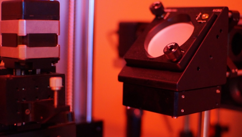
3D Printer

A demand for micron-scale resolution manufacturing traditionally limits the manufacturing means to 2D microfabrication techniques that are well developed in the micro-electronics industry; these microfabrication techniques employ a layer-by-layer fabrication scheme, which results in planar layouts (as opposed to 3D geometries). Alternatively, additive manufacturing (i.e., 3D printing) can create more complex geometries, however, micron-scale structures are limited to only polymeric materials; metal parts are only traditionally possibly at the macro-scale, hence a micron-scale multi-material scheme is not possible. Yet even at the macro-scale, laser-sintering metal 3D printing is a high temperature process which renders it incompatible with polymeric materials; this limitation further prohibits a multi-material manufacturing scheme in the 3D printing space. Additionally, chemical and/or physical metal coatings are all non-selective, which makes integration of metals with 3D printed micro-structures for electronic applications challenging, if not impossible. However, there are two conventional approaches for selectively incorporating metals into 3D printed dielectric structures: 1) Employing a 2D lithographic process: this is a non-trivial process when used on 3D surfaces. 2) Employing ink-jet (or aerosol-jet) printing to deposit metal particles on a surface: this technique is also challenging to use on a non-planar surface. Additionally, a deposited ink-jet metal layer has low adhesion quality to its underlaying substrate and it exhibits high electrical resistivity due to its polymer filler contamination— ~13 µΩ-cm (as opposed to high quality metal deposition with a low electrical resistivity— ~2 µΩ-cm). Therefore, employing any of these two approaches makes 3D printing no more an advantageous manufacturing process than conventional 2D microfabrication schemes.
DUJUD's fine grain proprietary 3D printers (40 nm resolution) are capable of fabricating micron-scale functional 3D electronic devices. Our 3D printers eliminate a need for any additional lithographic step while exhibiting exceptionally low metal resistivity (approx. 2.3 µΩ-cm) and semiconductor grade adhesion quality. This novel, first-of-its-kind scheme not only enables the formation of electronic circuits into a 3D geometry but also allows for the simple integration of pre-fabricated silicon dice in a monolithic fashion, hence little to no post-assembly process is needed. The technological foundation of the presented technology is commercially available and is currently being employed in different electronic applications.
